I am so thankful to everyone who attended this colloquium in the physics department at Colorado School of Mines. Our discussion began back in the 1880s with Hertz’s 1st observation and covered many practical aspects of photoelectron spectroscopy. In case anyone wants to look over the presentation, it’s here for you. Please cite it appropriately if you use any parts of it (as you see that I’ve done!). xps-colloquium-2016-web
Category: Photoelectron Spectroscopy
Dynamic Photoelectron Spectroscopy – a non-equilibrium technique

When one learns the rules of a particular approach, for the curious, it becomes a challenge to learn how to break them and to expand the limits. Since I’ve visited Dr. Cohen’s lab in Weizmann, my XPS experiments have presented me with too many opportunities for new directions. From electronically insulating ionic conductors to defect mediated photoconductivity in nanostructures, dynamics have been challenging me to think in new ways about XPS.
Many XPSers think of insulators as a nuisance that require charge neutralization to get any useful information at all. This perception stems from the persistent accumulation of photogenerated holes (+ charges) during continuous emission of X-ray generated photoelectrons. As these charges build up in the poorly conducting material, the surface potential shifts and the spectrometer’s Fermi level is no longer in equilibrium with the sample. In fact, a variety of other reasons can also account for non-equilibrium including heterojunction stabilized electron-hole pairs, thermal gradients and changing sample properties to name a few.
But really, why not measure insulators with XPS? We can learn so much about material interactions with charges, light and heat if we can model the non-equilibrium behavior. Actually, XPS is an ideal tool to assess the potential shifts during charging conditions. In principle, this is an electrostatics problem with well defined boundary conditions such as a fixed backplane via grounding and measurable surface potential via core level offsets. This is just what Dr. Hagai Cohen has been doing for nearly 20 years at Weizmann Institute to reveal properties of dielectrics for energy applications. In an older Nature paper summed up nicely in a news release, the reporter described the advantage of asymmetric potential profiling as deciphering what’s in a layered cake. As the sample is pushed further from equilibrium, the atomic constituents may reside along different segments in a potential gradient that depend on their location. By analyzing the core level shifts under non-equilibrium conditions, new things are informed. First, the atomic locations of elements relative to the sample surface are revealed. An extension into 3D provides a fantastic new approach for identifying locations of dopants or chemically heterogeneous nanostructures at the atomic scale. Further, when providing an external stimuli (light, electrons, heat, etc.), the nanoscale electronic responses can transform standard measurements (current-voltage, photoluminescence, etc.) into chemically resolved electrical responses. This gives a unique approach to evaluating functional nanostructures.
Dielectrics are particularly useful in this approach called Chemically Resolved Electrical Measurements (CREM) because they enhance the charging effect and enable generation of larger electrostatic fields during XPS. A great example of this is given by one of the most important solar energy heterojunctions, the silicon – silicon oxide heterojunction, which help provide electricity from many home’s roofs. In this case, CREM reveals the resilience of the insulating layer against electrical breakdown, a key metric for evaluating electronically active defects. This is a great example of not taking the current paradigm as static, but allowing one’s curiosity to guide the next steps.
If you are interested in CREM, XPS or anything about photoelectron spectroscopy, post a comment, drop me a line or get in the lab and try something new!
Happy XPSing!
A lesson in Ultraviolet Photoelectron Spectroscopy

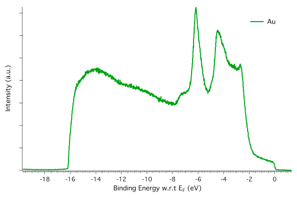
This fall, I had great fun teaching a graduate lecture at the Colorado School of Mines on the topic of Ultraviolet Photoelectron Spectroscopy (UPS). The first question I asked the students was “How many of you have taken some form of solid-state?” About half the hands went up. But for the lecture, we needed a bit more background. Very quickly we covered the band structure of metals and semiconductors, the Fermi energy and why these are so important for technology. What impromptu fun that was! At this point, we were able to really dive into UPS with diagrams and the key properties observable with UPS. I handed out data I had taken on gold and fullerene thin films. After explaining how to analyze the gold spectrum, students worked in groups of two and three. I attempted to view their learning experiences with fresh eyes and to encourage curiosity on the spectral details. After calculating the the work function and ionization energy of the separate materials, we constructed a band diagram for this hybrid heterostructure and enjoyed a brief discussion on the molecular structure of C60. The lesson outline and sample data are available here: UPS lesson (PPT).
